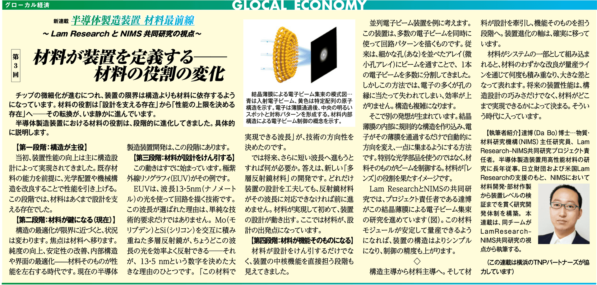
Entering the Realm of Atomic-Level Mechanisms
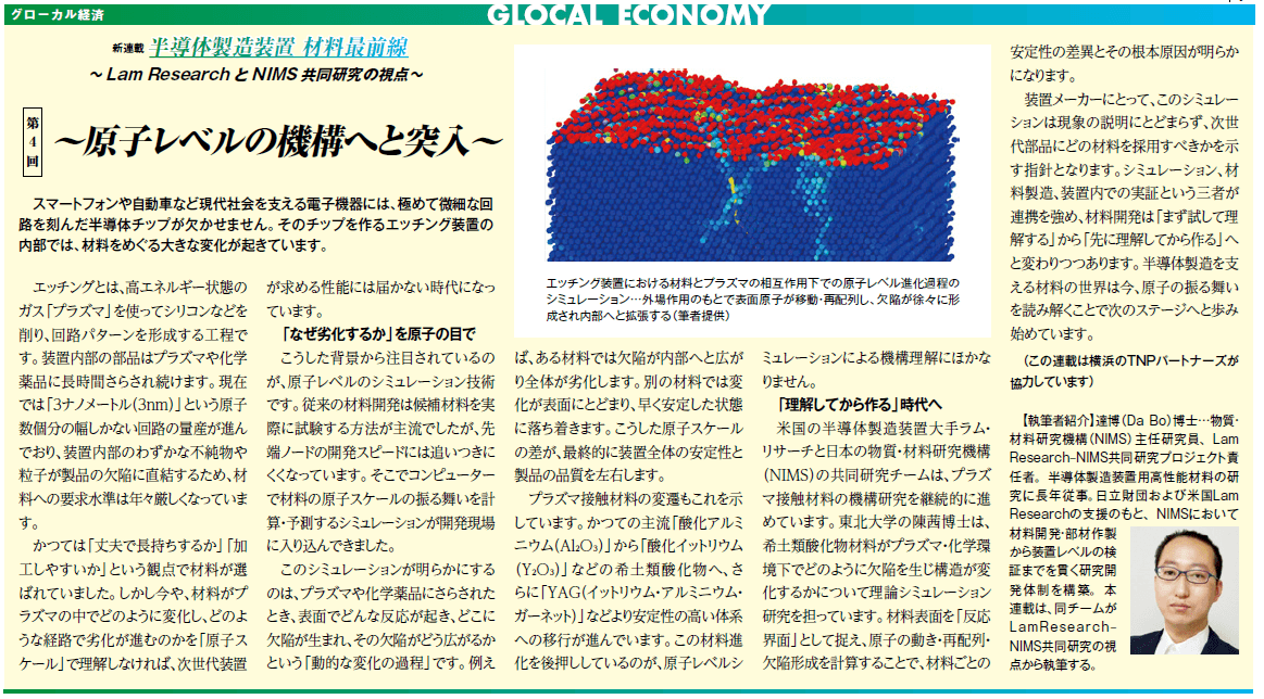
Electronic devices that support modern society, such as smartphones and automobiles, rely on semiconductor chips engraved with extremely fine circuits. Inside the etching equipment used to manufacture these chips, major changes regarding materials are taking place. Etching is a process that uses "plasma," a high-energy gas, to carve away silicon and other materials to form circuit patterns. Components inside the equipment are continuously exposed to plasma and chemicals for extended periods. Currently, with the mass production of "3 nanometer (3nm)" circuits—which are only a few atoms wide—underway, even minor impurities or particles inside the equipment can directly lead to product defects. Consequently, the standards required for materials are becoming stricter each year. In the past, materials were selected based on criteria such as "durability" and "ease of processing." Now, however, we have entered an era where failing to understand at the "atomic scale" how materials change within the plasma and the pathways through which degradation progresses means falling short of the performance required by next-generation equipment. ——Viewing "Why Degradation Occurs" Through an Atomic Lens Against this backdrop, atomic-level simulation technology is attracting attention. Traditional material development primarily relied on physically testing candidate materials, but this approach struggles to keep pace with the development speed of advanced nodes. Thus, simulations that use computers to calculate and predict the atomic-scale behavior of materials have found their way into the development site. What these simulations reveal is the "dynamic process of change"—what reactions occur on the surface, where defects originate, and how those defects spread when exposed to plasma or chemicals. For example, in one material, defects may spread inward, causing the entire structure to degrade. In another, changes may remain on the surface, quickly settling into a stable state. These atomic-scale differences ultimately determine the overall stability of the equipment and the quality of the product. The evolution of plasma-contact materials also illustrates this. There is an ongoing transition from the formerly mainstream "aluminum oxide" to rare-earth oxides like "yttrium oxide" and further to more highly stable systems such as "YAG (yttrium aluminum garnet)." What drives this material evolution is precisely the mechanistic understanding gained through atomic-level simulations. ——Moving Towards the Era of "Understand Before Making" A joint research team from major US semiconductor equipment manufacturer Lam Research and Japan's National Institute for Materials Science (NIMS) is continuously advancing mechanistic research on plasma-contact materials. Dr. Qian Chen of Tohoku University is leading theoretical simulation research on how rare-earth oxide materials develop defects and undergo structural changes in plasma and chemical environments. By treating the material surface as a "reaction interface" and calculating atomic movement, rearrangement, and defect formation, the differences in stability among materials and their root causes are revealed. For equipment manufacturers, this simulation goes beyond merely explaining phenomena; it serves as a guideline indicating which materials should be adopted for next-generation components. As the coordination among simulation, material manufacturing, and in-equipment verification strengthens, material development is shifting from "try first, understand later" to "understand first, make later." By deciphering atomic behavior, the world of materials supporting semiconductor manufacturing is now taking its first steps into the next stage. (This series is supported by TNP Partners in Yokohama)