Materials Define the Apparatus — The Changing Role of Materials
As chip miniaturization progresses, the limits of equipment are becoming more dependent on materials than on structure. The role of materials is shifting from "supporting the design" to "determining the upper limit of performance" – a transition that is quietly underway. The role of materials in semiconductor equipment has evolved in stages, as explained below.
——[Stage 1: Structure as the Protagonist]
Initially, improvements in equipment performance were mainly achieved through structural design. Performance was enhanced by refining optical layouts and mechanical structures, predicated on the capabilities of existing materials. In this stage, materials were merely an existence that supported the design.
——[Stage 2: Material Becomes the Key (Present)]
As structural optimization approaches its limits, the situation changes. The focus shifts to materials. This is an era where the material itself—through increased purity, improved stability, and optimization of internal structures and interfaces—dictates performance. Current semiconductor equipment development is in this stage.
——[Stage 3: Material Drives Design]
This movement has already begun. Extreme Ultraviolet Lithography (EUV) is an example. EUV is a technology that draws circuits using 13.5 nm (nanometer) wavelength light. The reason this wavelength was chosen was not just due to simple technical requirements. A major reason for deciding on the 13.5 nm figure is that multilayer mirrors, made by alternately stacking Molybdenum (Mo) and Silicon (Si), can efficiently reflect light at exactly this wavelength. The "wavelength achievable with this material" determined the direction of the technology.
In the future, what will be needed to move toward even shorter wavelengths? The answer is the development of new "multilayer mirror materials." No matter how much one refines the equipment design, if the mirror material cannot support that wavelength, no progress can be made. Equipment design only begins to move forward once the material is realized. Here, the material becomes the starting point of the design.
——[Stage 4: Material Becomes the Function Itself]
We are now seeing a stage where materials not only drive design but also directly take on the core functions of the equipment.
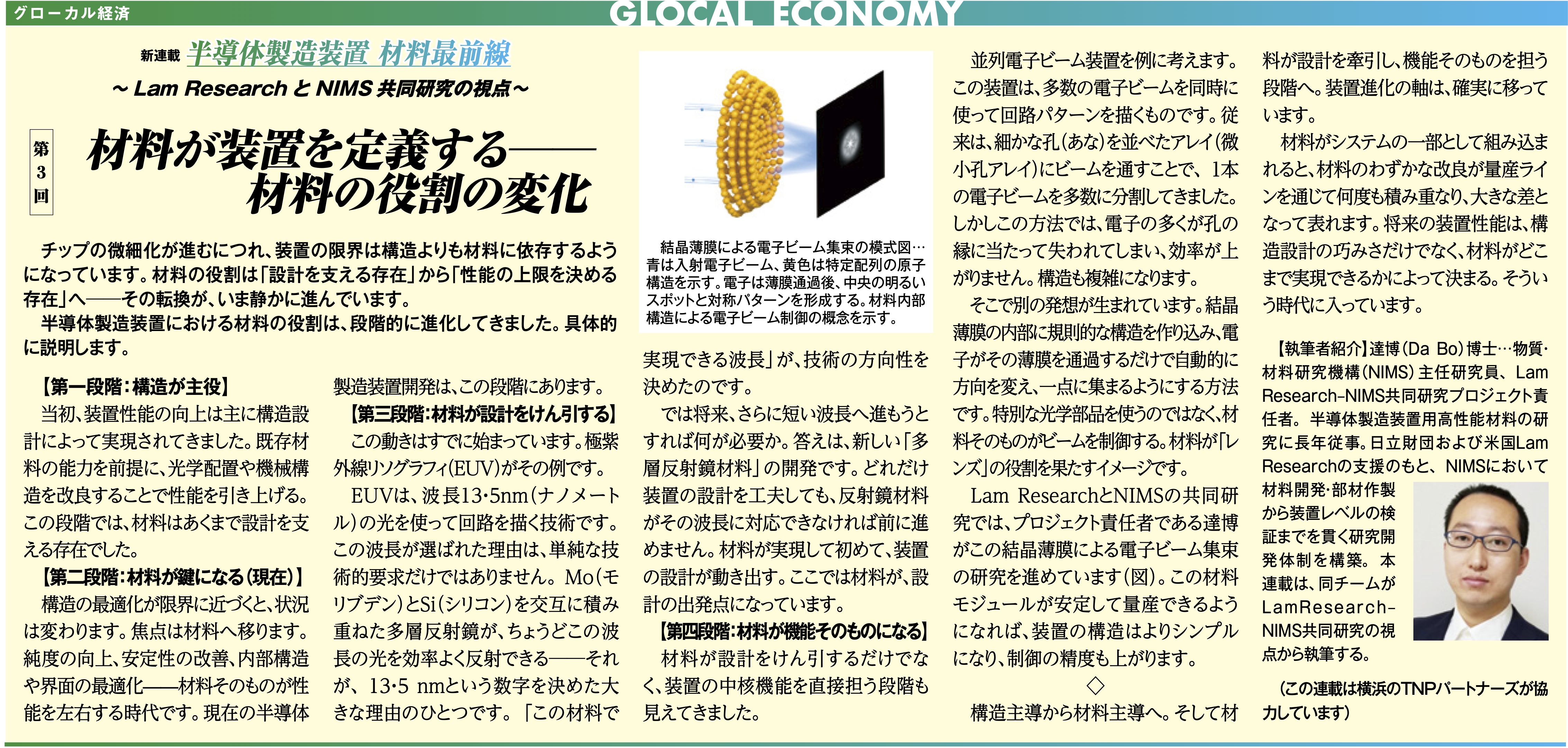
Take parallel electron beam (EB) equipment as an example. This apparatus draws circuit patterns using multiple electron beams simultaneously. Conventionally, a single electron beam was split into many by passing it through an array of fine apertures (micro-aperture array). However, in this method, many electrons are lost by hitting the edges of the holes, hindering efficiency and complicating the structure.
Hence, a different idea was born: creating a regular structure within a crystal thin film so that electrons automatically change direction and converge at a single point just by passing through the film. Instead of using special optical components, the material itself controls the electron beam. The concept is for the material to play the role of a "lens."
In the joint research between Lam Research and NIMS, project leader Dr. Bo Da is advancing research on this electron beam focusing using crystal thin films (Figure). If this material module can be stably mass-produced, equipment structures will become simpler and control precision will increase.
From structure-led to material-led. And then toward the stage where materials drive design and handle the functions themselves. The axis of equipment evolution is steadily shifting.
When a material is integrated as part of a system, slight improvements in the material accumulate repeatedly through mass production lines, resulting in a significant difference. Future equipment performance will be determined not only by the ingenuity of structural design but also by how far the materials can go. We have entered such an era.
Dr. Bo Da: Principal Researcher at the National Institute for Materials Science (NIMS) and leader of the Lam Research-NIMS Joint Research Project. He has long been engaged in research on high-performance materials for semiconductor equipment. Supported by the Hitachi Foundation and Lam Research (USA), he established a comprehensive R&D framework at NIMS spanning from material development and component fabrication to equipment-level validation. This series is written by the same team from the perspective of the Lam Research-NIMS joint research.