Breakthrough in Semiconductor Manufacturing Equipment:World's First Crystal for Precise Electron Beam Control
In recent years, semiconductors have increasingly taken on the character of an international strategic resource on par with oil, moving beyond their traditional role as the "rice of industry." Consequently, the importance of maintaining and expanding semiconductor manufacturing technologies and their supply chains is higher than ever. Against this backdrop, TNP Partners (Shin-Yokohama, Kohoku-ku, Yokohama), aiming to "build a Japanese version of Silicon Valley originating in Kanagawa Prefecture," continues to support semiconductor-related startups and researchers. For this feature, we interviewed Dr. Da Bo, Principal Investigator at the National Institute for Materials Science (NIMS), who is considered a promising candidate for a Nobel Prize. He has discovered a foundational technology that dramatically improves the performance of the electron beam equipment essential for miniaturizing semiconductor circuits. We asked him about the impact this innovative technology will have on semiconductor manufacturing.
—— Could you tell us about your research field?
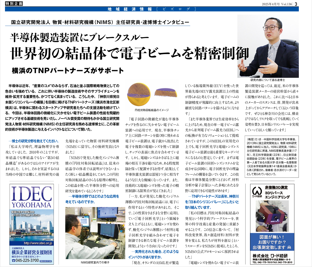
"During my university years, I majored in theoretical physics. In 2010, I came up with the idea that there might be a 'third crystal structure' that is neither a single crystal nor a quasicrystal. However, it was difficult to prove this in China at the time, so I went to study at the National Institute for Materials Science (NIMS), which was at the forefront of materials research, and later became a researcher there."
"The 'cylindrically symmetric rotational crystal' of indium oxide thin films that I discovered at NIMS has a completely new crystal structure that cannot be explained by conventional crystallographic systems. I am currently working on further elucidating the principles of this cylindrically symmetric rotational crystal and advancing applied research using this crystal in the semiconductor field."
—— What kind of applications are you considering in the semiconductor field?
"It is an application for electron beam equipment, which is indispensable for making semiconductor chips as electronic circuits become increasingly miniaturized. Currently, the electron beam equipment used to draw circuit patterns on semiconductor chips controls the electrons emitted from an electron gun using multiple electromagnetic lenses, focusing them on the surface of the chip. However, electromagnetic lenses are bulky, and to avoid mutual magnetic interference, they must be spaced apart to some extent. As a result, semiconductor lithography equipment has become a massive machine equivalent to the size of a room. Technologically, precision control of electrons using electromagnetic lenses is also reaching its limits."
"On the other hand, the cylindrically symmetric rotational crystal of the indium oxide thin film that I discovered has the property of interacting with electrons. Therefore, along with establishing a new field called 'electron diffraction optics' to apply this property to various areas, we headed in the direction of developing a novel electron beam system that controls electrons by combining the indium oxide thin film material with electron diffraction optics, without using electromagnetic lenses."
—— What impact will it have if it is commercialized?
"I believe it can achieve performance surpassing the world's most advanced EUV (Extreme Ultraviolet) lithography equipment currently manufactured by ASML in the Netherlands. Because the control precision of the electron beam will dramatically improve, we will be able to draw much finer circuit patterns."
"Furthermore, in the semiconductor industry, transitioning from current single electron beam lithography to multiple electron beam lithography (MEBL) is advocated as a strong solution to further increase production efficiency. We anticipate that electron diffraction optics and electromagnetic lens-less electron beam equipment will become the most critical key devices in commercializing this MEBL. First, we will urgently complete the diffraction lens system for the electron beam equipment while simultaneously constructing the theoretical framework for electron diffraction optics. This technology has the potential for applications not limited to semiconductor manufacturing, but extending to diverse fields such as materials analysis and quantum computing."
—— TNP Partners has been working for many years to make Kanagawa the "Silicon Valley of Japan."
"My goal is to have the scientific breakthrough of discovering the cylindrically symmetric rotational crystal contribute to the development of global science and technology and industry. Based on this belief, I proposed the slogan 'Materials change the world, and we create the materials' to NIMS, and it was adopted for their official promotion."
"Regarding the development of electron beam equipment that doesn't use electromagnetic lenses, top executives from a U.S. semiconductor manufacturing equipment maker recently contacted me directly. In contrast, the stance of Japanese manufacturers gives the impression that they all wait to approach us until the development is fully completed. I sincerely hope that companies in Kanagawa will not just follow the crowd, but instead maintain a posture of taking on challenges even at a risk, to bring the Japanese version of Silicon Valley to life."
Supported by TNP Partners in Yokohama
Da Bo... After graduating from the University of Science and Technology of China, he joined the National Institute for Materials Science (NIMS) in 2013. He was appointed as a Researcher in 2016 and promoted to Principal Investigator in 2019. He is a recipient of the NIMS President's Progress Award (2017), the Kao Science Incentive Award (2022), and the Kurata Grant from the Hitachi Global Foundation (2023). Highly acclaimed by Professor Emeritus Ryuichi Shimizu of Osaka University (former Chair of the 141st Committee of the Japan Society for the Promotion of Science), a leading figure in the electron beam industry, Dr. Da is regarded as his successor and the leader of the "Shimizu school."