From Transistors to Key Materials
Semiconductor manufacturing technology has now entered the realm of the atomic level. Along with this shift, the focus of development has changed. Previously, transistor design played the leading role, but today, "Key Materials" have taken center stage. These are materials that must operate stably over long periods within manufacturing equipment, even while exposed to high temperatures, high vacuums, and intense electromagnetic fields. The quality of these materials now significantly dictates semiconductor performance.
——Manipulating the Needle Tip
To leverage atomic-level manufacturing technology, one must first identify exactly "where the performance is determined" within a material. In fact, performance is governed by what are called "Key Sites"—specific locations where a very small number of atoms play a specialized role. There is a growing demand for a mindset that improves these key sites at the atomic level to enhance the performance of the entire equipment and, by extension, the entire production line.
A prime example is the "Cold Field Emission (CFE) Electron Source" used in inspection and metrology equipment. In semiconductor factories, electron beams are used to detect minute line widths and defects on wafers. The performance depends on the quality of the "electron source," which functions much like a light bulb component.
A CFE electron source works by applying a strong electric field to an extremely fine needle tip made of a single crystal to extract electrons. It is considered the superior technology today because it provides a bright and stable electron beam.
In this field, Ryuichi Shimizu conducted pioneering research starting in the 1970s, challenging the development of "Cold Field Emission Cathodes" using materials such as Lanthanum Hexaboride (LaB₆). The crucial point here is that the brightness, stability, and lifespan of the electron beam are not determined by the average properties of the bulk material, but by the atomic arrangement of just a few to several dozen atoms at the very tip of the needle. Even a slight difference in how these atoms are aligned creates a massive disparity in image clarity and measurement precision.
In recent years, atomic-level manufacturing technology has made it possible to process these needle tips directly. In the Lam Research–NIMS joint research project led by Dr. Da Bo's research group, Dr. Taiqiang Zhang, who is in charge of metal boride electron sources, is developing a new method using atomic manipulation tools. Specifically, the surface of the needle tip is treated as a "workbench," where lanthanum atoms are moved and stacked one by one at the tip to assemble an atomic cluster of a precisely designed shape and size.
——From Electron Sources to Improved Yield
If the electron source is stable and can emit a bright, low-noise beam, the performance of the entire inspection and metrology system improves. In advanced processes, defects are becoming increasingly small and difficult to see; however, finding them quickly and accurately reduces trial and error and raises the yield to mass-production levels. Organizing just a few atoms leads to better equipment performance, improved manufacturing processes, and progress for the entire industry. The CFE electron source is a perfect example that clearly demonstrates the value of atomic-level manufacturing.
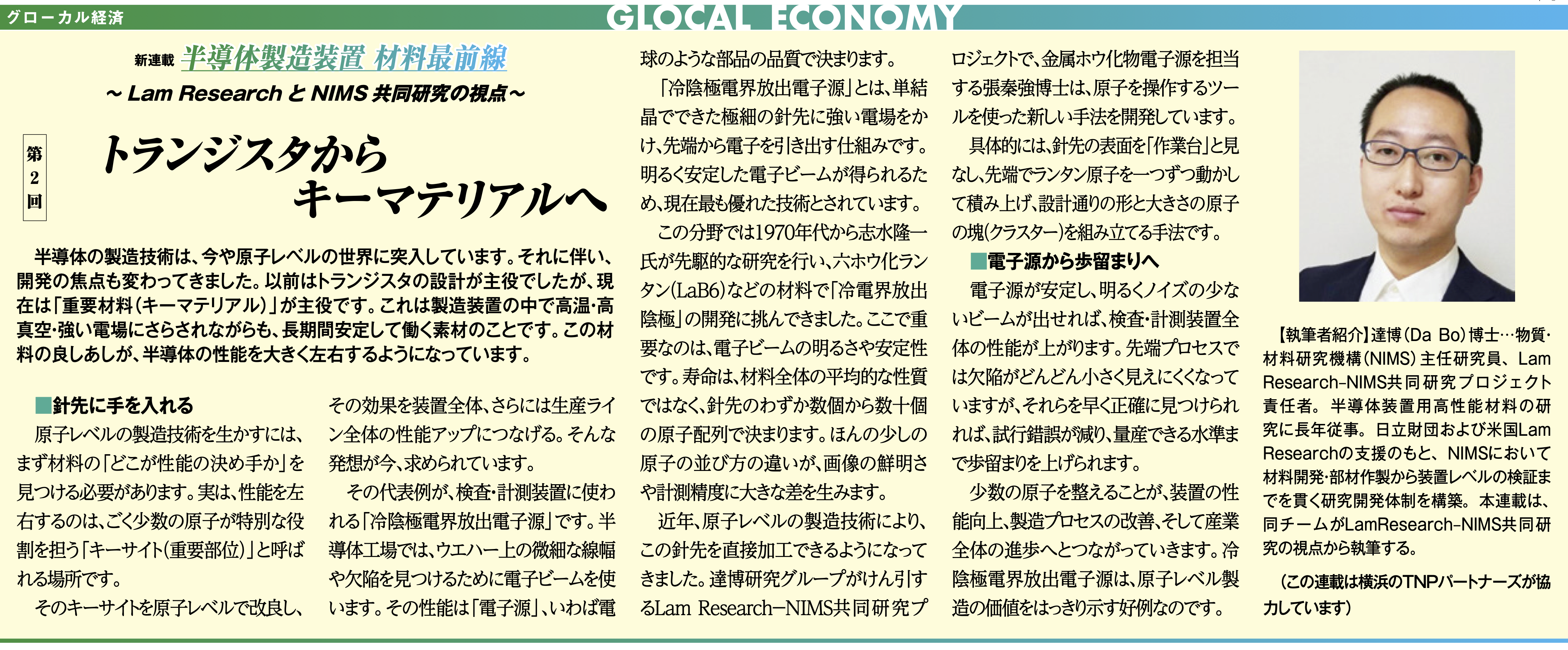
Dr. Da Bo Principal Researcher at the National Institute for Materials Science (NIMS) and Leader of the Lam Research-NIMS Joint Research Project. He has been engaged in the research of high-performance materials for semiconductor equipment for many years. With support from the Hitachi Foundation and Lam Research (USA), he has established an R&D framework at NIMS that spans from materials development and component fabrication to equipment-level verification. This series is authored by his team from the perspective of the Lam Research-NIMS joint research.